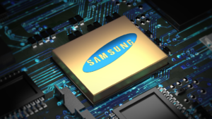
Seoul/San Jose — Reuters — Samsung Electronics, the world’s top memory chip maker, has been pushing a new business initiative in contract manufacturing in an effort to boost production of artificial intelligence (AI) chips. Structurally incorporating its lead system semiconductors—memory, chip foundry, and chip packaging—into play to meet nascent demand for AI, Samsung keeps charging forward.
By facilitating communication and collaboration between the memory chip team, the foundry team, and the packaging team, Samsung succeeded in reducing production time for AI chips by about 20%, the company announced Wednesday. “We are really living in the age of AIs; the dawn of generative AI is totally changing the landscape of technology,” said Siyoung Choi, President and General Manager of the Foundry Business, speaking at a Samsung event in San Jose, California. According to Choi, Samsung forecasts that worldwide chip industry revenues could rise to $778 billion by 2028, driven by fast-growing demand for AI chips. Executive Vice President and Foundry Sales and Marketing head, Marco Chisari, agreed with estimates by OpenAI CEO Sam Altman of growing demand for AI chips at a briefing ahead of the event. Altman has lately been showing interest in building many new chip factories, Reuters reported.
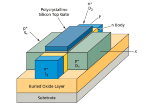
This unique position, which Samsung holds as a memory chip supplier, foundry service provider, and chip designer all under one roof, has always been a double-edged sword. Some customers were suspicious of working with the foundry unit of Samsung out of fear of possible conflicts of interest. Now, with the current boom of AI chips, highly integrated chip components are needed in processing large data volumes at faster rates; therefore, the comprehensive approach taken by Samsung is vital in strategy. Therefore, it also introduced a new gate-all-around (GAA) transistor structure that promises to deliver significant improvements in both performance per watt.
Though this technology, called GAA-based chips, is in the works by rivals such as TSMC, too, early adoption has been by Samsung, which plans to mass-produce its second-generation 3-nanometer chips using GAA in the latter half of this year.
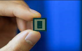
Samsung also announced a second generation processor called G4FET. It placed, for the first time, an ingenious power rail on the backside of the wafer to enhance the power delivery, with volume production to start in 2027.
Conclusion
“Samsung, with its integrated AI chip manufacturing strategically linked to memory chips, foundry, and packaging services, contends for the rapidly growing AI market. The strategy optimizes production schedules, ensuring that new technologies, such as Gate-All-Around architecture, are used in the production of high-performance AI chips on a large scale. This effort would further study and help in technological advancement with an added goal of regaining a position of leadership for Samsung in the global chip industry. “.